The technology industry continues to be a hotbed of innovation, driven by widespread adoption of Internet of Things (IoT) devices, the increasing demand for high-quality semiconductor devices, the need for efficient and reliable defect detection, and the growing importance of technologies such as machine learning, computer vision, and image processing. In the last three years alone, there have been over 3.6 million patents filed and granted in the technology industry, according to GlobalData’s report on Innovation in Internet of Things: Wafer defect inspection system. Buy the report here.
Smarter leaders trust GlobalData

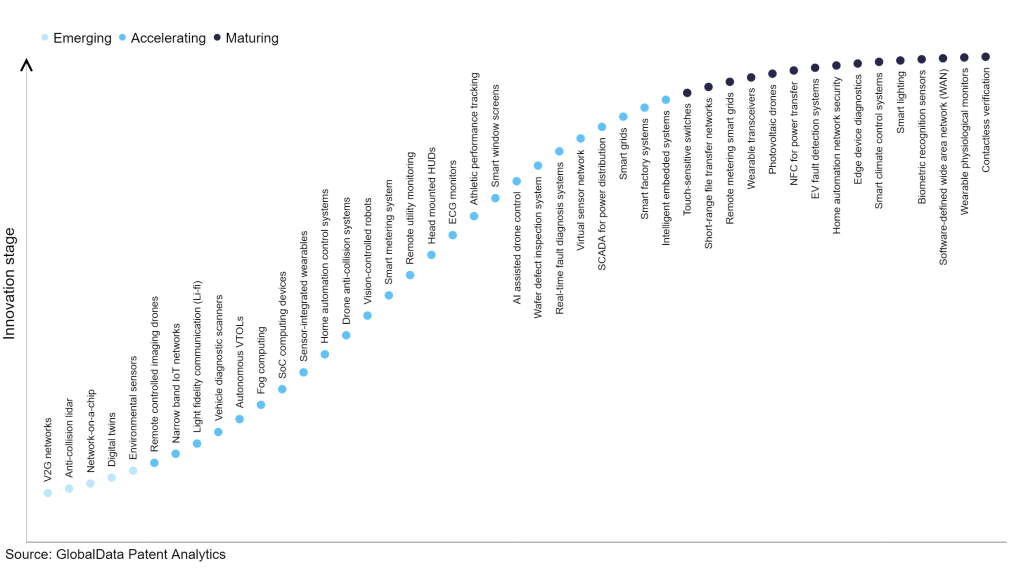
However, not all innovations are equal and nor do they follow a constant upward trend. Instead, their evolution takes the form of an S-shaped curve that reflects their typical lifecycle from early emergence to accelerating adoption, before finally stabilising and reaching maturity.
Identifying where a particular innovation is on this journey, especially those that are in the emerging and accelerating stages, is essential for understanding their current level of adoption and the likely future trajectory and impact they will have.
300+ innovations will shape the technology industry
According to GlobalData’s Technology Foresights, which plots the S-curve for the technology industry using innovation intensity models built on over 2.5 million patents, there are 300+ innovation areas that will shape the future of the industry.
Within the emerging innovation stage, environmental sensors, digital twins, and network-on-a-chip are disruptive technologies that are in the early stages of application and should be tracked closely. Intelligent embedded systems, smart factory systems, and smart grids are some of the accelerating innovation areas, where adoption has been steadily increasing. Among maturing innovation areas are contactless verification, wearable physiological monitors, and software defined wide area network, which are now well established in the industry.
Innovation S-curve for IoT in the technology industry
Wafer defect inspection system is a key innovation area in IoT
The wafer defect inspection system employs automated optical inspection technology to identify and categorise defects on semiconductor wafers. It is capable of detecting various types of defects, including particle contamination, surface damage, scratches, and pinholes. This system offers manufacturers a detailed analysis of the wafer's surface, facilitating prompt identification and resolution of process-related concerns that could otherwise result in expensive product failures.
GlobalData’s analysis also uncovers the companies at the forefront of each innovation area and assesses the potential reach and impact of their patenting activity across different applications and geographies. According to GlobalData, there are 40+ companies, spanning technology vendors, established technology companies, and up-and-coming start-ups engaged in the development and application of wafer defect inspection system.
Key players in wafer defect inspection system – a disruptive innovation in the technology industry
‘Application diversity’ measures the number of different applications identified for each relevant patent and broadly splits companies into either ‘niche’ or ‘diversified’ innovators.
‘Geographic reach’ refers to the number of different countries each relevant patent is registered in and reflects the breadth of geographic application intended, ranging from ‘global’ to ‘local’.
Patent volumes related to wafer defect inspection system
Source: GlobalData Patent Analytics
KLA is a leading patent filer in wafer defect inspection systems. One of the company's patents focuses on determining characteristics of a pattern of interest on a specimen. The patent describes methods and systems for acquiring and analysing output from an inspection system without detecting defects. This enables the selection of instances of the pattern of interest. The system then acquires output from an output acquisition subsystem for the selected instances and determines the characteristics of the pattern of interest based on this acquired output.
Other prominent patent filers in the space include Toshiba and Hitachi.
By geographic reach, Fogale Nanotech leads the pack, followed by Peter Rose and DAIHEN. In terms of application diversity, Kulicke & Soffa Industries holds the top position, followed by Fogale Nanotech and Rambus.
The wafer defect inspection system is an IoT innovation that utilises advanced technologies to inspect and detect defects in semiconductor wafers during the manufacturing process. This system plays a crucial role in ensuring the quality and reliability of integrated circuits.
To further understand how IoT is disrupting the technology industry, access GlobalData’s latest thematic research report on Internet of Things – Thematic Research.
Data Insights
From
![]()
The gold standard of business intelligence.
Blending expert knowledge with cutting-edge technology, GlobalData’s unrivalled proprietary data will enable you to decode what’s happening in your market. You can make better informed decisions and gain a future-proof advantage over your competitors.
GlobalData, the leading provider of industry intelligence, provided the underlying data, research, and analysis used to produce this article.
GlobalData’s Patent Analytics tracks patent filings and grants from official offices around the world. Textual analysis and official patent classifications are used to group patents into key thematic areas and link them to specific companies across the world’s largest industries.