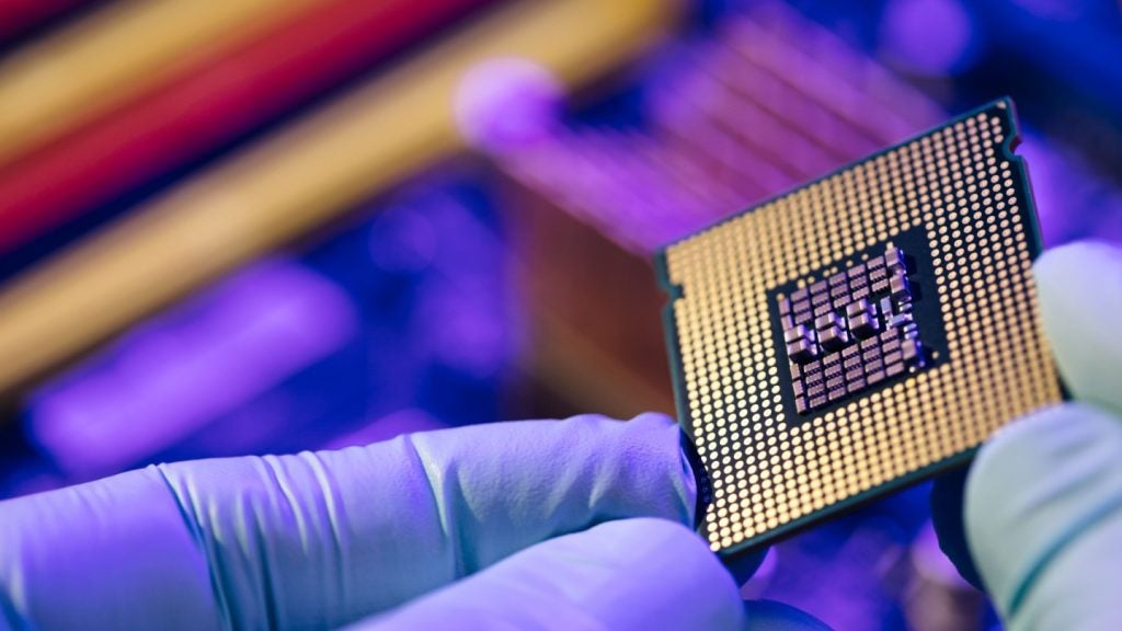
Jenoptik has patented a method for testing optoelectronic chips on a wafer, involving precise alignment of electrical and optical interfaces. The process includes adjusting the wafer in three steps to ensure optimal contact and alignment, enabling the routing of electrical and optical signals for testing. GlobalData’s report on Jenoptik gives a 360-degree view of the company including its patenting strategy. Buy the report here.
Smarter leaders trust GlobalData

According to GlobalData’s company profile on Jenoptik, Lidar for weather forecasting was a key innovation area identified from patents. Jenoptik's grant share as of February 2024 was 48%. Grant share is based on the ratio of number of grants to total number of patents.
Method for testing optoelectronic chips on wafer with specific alignment

A recently granted patent (Publication Number: US11906579B2) discloses a method for testing optoelectronic chips on a wafer, involving a positioning table and a contacting module with electrical and optical interfaces. The method includes precise alignment of optical deflection elements with optical interfaces, followed by routing of electrical and optical signals through the interfaces associated with each other. The alignment process involves adjusting the positioning table in the X and Y directions to achieve maximum optical signal intensity, and subsequently deflecting the chips in the X-Y direction based on the coupling angle of the optical deflection element before final positioning in the Z direction.
Furthermore, the patent claims include additional features such as storing the offset resulting from the initial and subsequent adjustment positions for further chip adjustments, monitoring and correcting the optical working distance to maintain the predefined pressing force, and replacing needles in the contacting module when the optical working distance falls below a predetermined minimum distance. Additionally, the method involves ensuring that the optical signals over-radiate the interface when coupled and have a specific radiation intensity distribution when entering the interfaces. These claims highlight the comprehensive nature of the testing method, ensuring accurate alignment and signal routing for optoelectronic chips on a wafer, ultimately improving the efficiency and reliability of the testing process.
To know more about GlobalData’s detailed insights on Jenoptik, buy the report here.
Premium Insights
From
![]()
The gold standard of business intelligence.
Blending expert knowledge with cutting-edge technology, GlobalData’s unrivalled proprietary data will enable you to decode what’s happening in your market. You can make better informed decisions and gain a future-proof advantage over your competitors.
GlobalData, the leading provider of industry intelligence, provided the underlying data, research, and analysis used to produce this article.
GlobalData Patent Analytics tracks bibliographic data, legal events data, point in time patent ownerships, and backward and forward citations from global patenting offices. Textual analysis and official patent classifications are used to group patents into key thematic areas and link them to specific companies across the world’s largest industries.