Nanoelectronics, the use of nanotechnology in electronic components, has huge potential to develop faster and more energy efficient electronic devices.
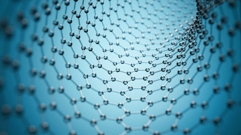
This area of technology relies on the development of nanomaterials, and one material that has shown promise in this area is graphene. Only one atom thick, graphene is excellent for conducting electrical current and heat, and is often referred to as a “miracle material”.
Go deeper with GlobalData


Access deeper industry intelligence
Experience unmatched clarity with a single platform that combines unique data, AI, and human expertise.
However, although graphene has the potential to be used in electronics, photonics or sensors, it is very difficult to engineer the electrical properties.
As the material is so thin, tiny irregularities in the pattern can alter its properties. For example, it is difficult, is to induce a bandgap, which is crucial for making transistors and optoelectronic devices.
Towards nanoelectronics
In order to harness the potential of the material in nanoelectronics, The Center for Nanostructured Graphene at The Technical University of Denmark and Aalborg University was established in 2012 specifically to study how the properties of graphene can be engineered.
They have studied how the properties of graphene can be engineered in different ways, such as making a very fine pattern of holes. This should subtly change the quantum nature of the electrons in the material, and allow the properties of graphene to be tailored. However, doing this can mean that the material no longer behaves like graphene.
Peter Bøggild, a professor at DTU Physics, explains why this happens:
“When you make patterns in a material like graphene, you do so in order to change its properties in a controlled way – to match your design. However, what we have seen throughout the years is that we can make the holes, but not without introducing so much disorder and contamination that it no longer behaves like graphene. It is a bit similar to making a water pipe, with a poor flow rate because of coarse manufacturing. On the outside, it might look fine. For electronics, that is obviously disastrous.”
Now, the team of researchers believe they have solved the problem. First, two postdocs from DTU Physics encapsulated graphene inside another two-dimensional material called hexagonal boron nitride, a non-conductive material that is often used for protecting graphene’s properties.
Next, they used a technique called electron beam lithography to carefully pattern the protective layer of boron nitride and graphene below with a pattern of ultra-small holes.
The roughness at the edge of the holes is less than 1 nanometer or a billionth of a metre and this level of precision means that the properties can be controlled. This allows 1000 times more electrical current to flow than had been reported in such small graphene structures.
Peter Bøggild explains what this means for the use of graphene in nanoelectronics:
“Many scientists had long since abandoned attempting nanolithography in graphene on this scale, and it is quite a pity since nanostructuring is a crucial tool for exploiting the most exciting features of graphene electronics and photonics. Now we have figured out how it can be done; one could say that the curse is lifted. There are other challenges, but the fact that we can tailor electronic properties of graphene is a big step towards creating new electronics with extremely small dimensions.”