Anderon, a subsidiary of IBM, has finalised a $1bn award agreement with the US Department of Commerce (DoC) under the CHIPS and Science Act.
The funding is aimed at accelerating research and development (R&D) activities for Anderon’s pure-play quantum wafer foundry based in Albany, New York.
Go deeper with GlobalData


Access deeper industry intelligence
Experience unmatched clarity with a single platform that combines unique data, AI, and human expertise.
The deal, first announced under a letter of intent in May, is intended to enhance the nation’s quantum wafer manufacturing capabilities.
The CHIPS award will be matched by an additional $1bn investment from IBM, further supporting Anderon’s operations as a specialised 300mm quantum wafer foundry.
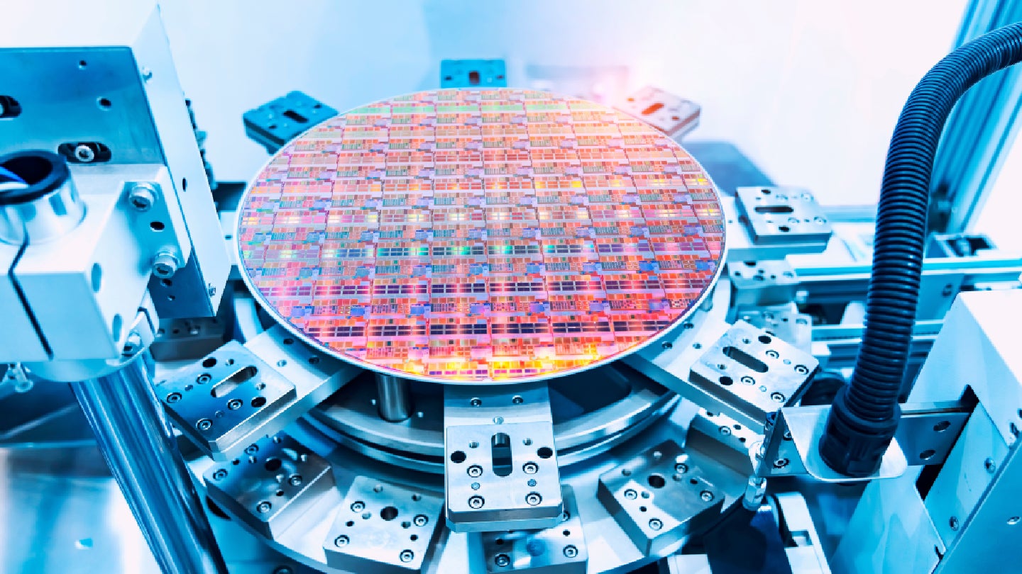
Anderon serves the quantum industry by manufacturing wafers for a broad range of customers.
The facility’s offerings include wafers that support superconducting qubit arrays, as well as quantum input/output signalling and readout signal chain components.
According to IBM, these technologies are foundational for a diverse set of quantum computing architectures, with additional modalities planned for future development.
IBM said that Anderon has already achieved a key operational milestone, with the initial batch of quantum wafers now running through its manufacturing process. This marks the transition of advanced pre-production research into commercial-grade quantum wafer technologies.
Anderon CEO Mukesh Khare said: “This agreement with the Department of Commerce strengthens our ability to deliver the manufacturing scale the quantum industry needs. We’re building a foundation that will let quantum move from research breakthroughs to real-world impact.”
Anderon aims to support the advancement of the quantum sector, emphasising the importance of scalable manufacturing for technology development, supply chain resilience, and the growth of the wider quantum ecosystem.
IBM Research director and IBM Fellow Jay Gambetta said: “IBM’s quantum roadmap requires a manufacturing foundation that can scale at the pace our work demands. Anderon’s focus on wafer fabrication gives us exactly that and strengthens our ability to execute and accelerate progress toward the next era of quantum computing.”
In July 2026, GlobalFoundries entered into a letter of intent with the US DoC for an anticipated $300m award to boost research and development in silicon photonics.
The expected funding is part of the Department’s CHIPS R&D Office programmes and is intended to advance work on optical materials, wafer technologies, and advanced packaging.