The technology industry continues to be a hotbed of patent innovation. Activity is driven by the increasing demand for high-quality integrated circuits, advancements in inspection techniques, and the continuous miniaturization of semiconductor devices, and growing importance of technologies such as optical inspection, electron microscopy, and various non-destructive testing methods. These technologies enable manufacturers to identify and address defects early in the production process, leading to improved yield rates and higher quality semiconductor products. In the last three years alone, there have been over 4.1 million patents filed and granted in the technology industry, according to GlobalData’s report on Innovation in technology: wafer defect inspection. Buy the report here.
Smarter leaders trust GlobalData

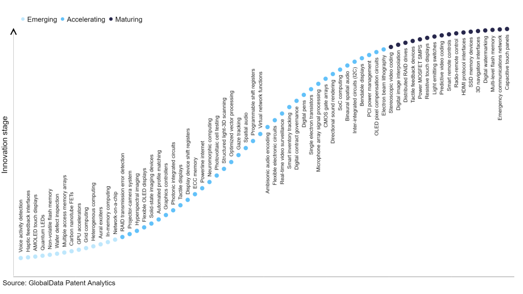
However, not all innovations are equal and nor do they follow a constant upward trend. Instead, their evolution takes the form of an S-shaped curve that reflects their typical lifecycle from early emergence to accelerating adoption, before finally stabilizing and reaching maturity.
Identifying where a particular innovation is on this journey, especially those that are in the emerging and accelerating stages, is essential for understanding their current level of adoption and the likely future trajectory and impact they will have.
190+ innovations will shape the technology industry
According to GlobalData’s Technology Foresights, which plots the S-curve for the technology industry using innovation intensity models built on over 1.5 million patents, there are 190+ innovation areas that will shape the future of the industry.
Within the emerging innovation stage, network-on-a-chip, in-memory computing, and aural exciters are disruptive technologies that are in the early stages of application and should be tracked closely. Electron beam lithography, OLED pixel compensation circuits, and PCI power management are some of the accelerating innovation areas, where adoption has been steadily increasing. Among maturing innovation areas are capacitive touch panels and emergency communications network, which are now well established in the industry.
Innovation S-curve for the technology industry
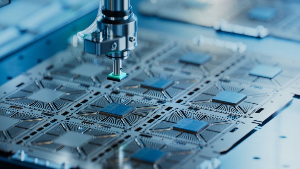
Wafer defect inspection is a key innovation area in technology
Wafer defect inspection is the critical examination of semiconductor wafers to pinpoint and assess any irregularities or flaws in their structure or composition. This process is paramount in guaranteeing the performance and quality of semiconductor devices and components produced from these wafers. Diverse approaches and systems, including the application of structured light patterns and advanced imaging methods, are deployed to evaluate characteristics like adhesive material properties, identify polishing discrepancies, and scrutinize internal fractures within wafers. Furthermore, systems for wafer alignment and computational analysis aid in accurate defect classification and positioning.
GlobalData’s analysis also uncovers the companies at the forefront of each innovation area and assesses the potential reach and impact of their patenting activity across different applications and geographies. According to GlobalData, there are 90+ companies, spanning technology vendors, established technology companies, and up-and-coming start-ups engaged in the development and application of wafer defect inspection.
Key players in wafer defect inspection – a disruptive innovation in the technology industry
‘Application diversity’ measures the number of applications identified for each patent. It broadly splits companies into either ‘niche’ or ‘diversified’ innovators.
‘Geographic reach’ refers to the number of countries each patent is registered in. It reflects the breadth of geographic application intended, ranging from ‘global’ to ‘local’.
Patent volumes related to wafer defect inspection
| Company | Total patents (2010 - 2022) | Premium intelligence on the world's largest companies |
| Kulicke & Soffa Industries | 9 | Unlock Company Profile |
| Disco | 32 | Unlock Company Profile |
| IMEC, VZW | 9 | Unlock Company Profile |
| Topcon | 8 | Unlock Company Profile |
| Lam Research | 19 | Unlock Company Profile |
| KLA | 1254 | Unlock Company Profile |
| Sumco | 12 | Unlock Company Profile |
| Daifuku | 7 | Unlock Company Profile |
| Taiwan Semiconductor Manufacturing | 100 | Unlock Company Profile |
| Fraunhofer-Gesellschaft zur Forderung der Angewandten Forschung | 9 | Unlock Company Profile |
| Camtek | 29 | Unlock Company Profile |
| Hoya | 16 | Unlock Company Profile |
| Soitec | 9 | Unlock Company Profile |
| Semiconductor Manufacturing International | 12 | Unlock Company Profile |
| Hitachi | 249 | Unlock Company Profile |
| Peter Rose | 8 | Unlock Company Profile |
| Applied Materials | 237 | Unlock Company Profile |
| Canon | 11 | Unlock Company Profile |
| ASML | 87 | Unlock Company Profile |
| Screen | 15 | Unlock Company Profile |
| Sumitomo Chemical | 7 | Unlock Company Profile |
| IBM | 8 | Unlock Company Profile |
| Tokyo Electron | 173 | Unlock Company Profile |
| Toshiba | 224 | Unlock Company Profile |
| Hamamatsu Photonics KK | 15 | Unlock Company Profile |
| Micron Technology | 14 | Unlock Company Profile |
| Shanghai Micro Electronics Equipment | 8 | Unlock Company Profile |
| Fogale Nanotech | 11 | Unlock Company Profile |
| Park Systems Corp. | 7 | Unlock Company Profile |
| Kioxia | 15 | Unlock Company Profile |
| ChangXin Memory Technologies | 11 | Unlock Company Profile |
| Unity Semiconductor | 10 | Unlock Company Profile |
| The French Alternative Energies and Atomic Energy Commission | 11 | Unlock Company Profile |
Source: GlobalData Patent Analytics
Among the companies innovating in wafer defect inspection, KLA is one of the leading patents filers. The company’s patent describes the methods and systems that facilitate the setup of specimen inspection by employing design and noise-based care areas. A system comprises computer subsystems tasked with creating a design-based care area for a specimen, as well as determining specific output attributes for multiple instances of the care area on the specimen using data acquired from an output acquisition subsystem. These computer subsystems further partition the multiple instances of the care area on the specimen into distinct care area sub-groups exhibiting statistically varying values of the output attribute(s), and then select a parameter for an inspection recipe tailored to the specimen based on these distinct care area sub-groups. Other prominent patent filers in the space include Hitachi and Applied Materials.
In terms of application diversity, Kulicke & Soffa Industries leads the pack, while Fogale Nanotech and Daifuku stood in second and third positions, respectively. By means of geographic reach, Semiconductor Manufacturing International held the top position, followed by Fogale Nanotech and KLA.
Wafer defect inspection plays a critical role in semiconductor manufacturing, ensuring the quality and reliability of electronic components. By meticulously identifying and analysing defects in semiconductor wafers, this process helps maintain high production standards, ultimately leading to the creation of more reliable and efficient electronic devices.
To further understand the key themes and technologies disrupting the technology industry, access GlobalData’s latest thematic research report on Technology.
Premium Insights
From
![]()
The gold standard of business intelligence.
Blending expert knowledge with cutting-edge technology, GlobalData’s unrivalled proprietary data will enable you to decode what’s happening in your market. You can make better informed decisions and gain a future-proof advantage over your competitors.
GlobalData, the leading provider of industry intelligence, provided the underlying data, research, and analysis used to produce this article.
GlobalData’s Patent Analytics tracks patent filings and grants from official offices around the world. Textual analysis and official patent classifications are used to group patents into key thematic areas and link them to specific companies across the world’s largest industries.