Sony Semiconductor Solutions and Taiwan Semiconductor Manufacturing Company (TSMC) have unveiled plans to form a strategic partnership in next-generation image sensors.
The parties have signed a non-binding memorandum of understanding (MOU).
Go deeper with GlobalData


Access deeper industry intelligence
Experience unmatched clarity with a single platform that combines unique data, AI, and human expertise.
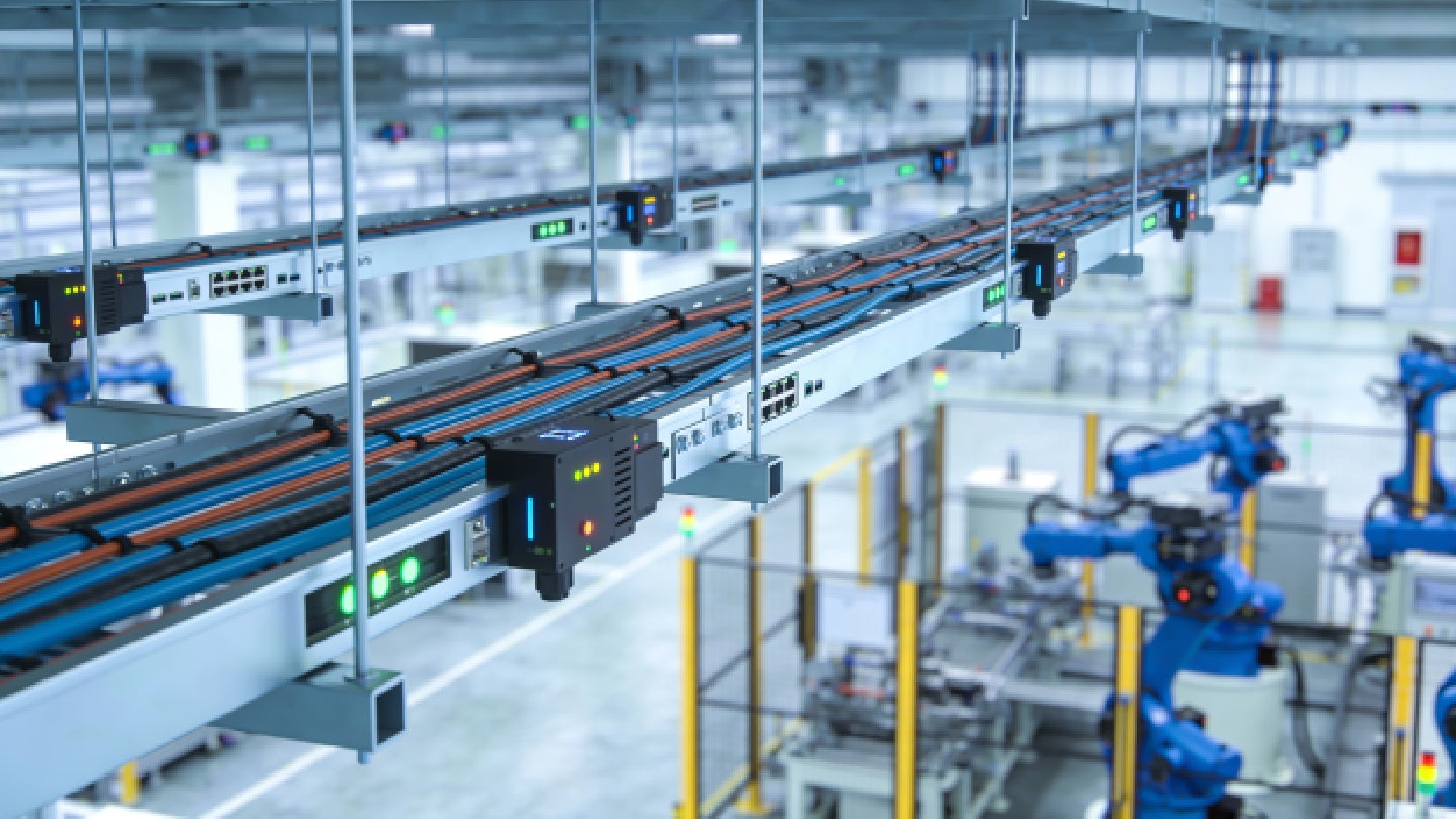
According to the two companies, plans are underway to form a joint venture (JV), with Sony Semiconductor Solutions holding the majority and controlling interest. The venture aims to establish development and manufacturing lines at Sony Semiconductor Solutions’ newly built semiconductor fabrication plant in Koshi City, Kumamoto Prefecture, Japan.
The joint venture would bring together Sony Semiconductor Solutions’ image sensor design and TSMC’s advanced semiconductor process technology to enhance the development and manufacturing of high-performance image sensors.
TSMC senior vice president and deputy co-chief operating officer Kevin Zhang said: “This partnership underscores our shared commitment and mutual vision of leveraging cutting-edge technologies and innovative solutions to deliver leading sensing technology and products. We look forward to working closely together to achieve impactful results and create lasting value for all stakeholders.”
The two companies are in discussions regarding potential investments to be made by the joint venture, with further capital investment by Sony also being considered for its existing Nagasaki plant. These investments would be made in phases in response to market demand and would depend on support from the Japanese government.
Furthermore, the incorporation of the joint venture is contingent on the signing of a definitive legally binding agreement and the meeting of the usual closing conditions.
Both Sony Semiconductor Solutions and TSMC are aiming to strategically position themselves to supply image sensors for emerging sectors. These include AI, automotive technology, and robotics, responding to rapidly evolving technology requirements across industries.
The new venture is expected to create opportunities for leveraging both companies’ expertise. Sony Semiconductor Solutions intends to contribute its sensor design experience while TSMC will supply manufacturing and process capability.
Sony Semiconductor Solutions president and CEO Shinji Sashida said: “This JV is a significant initiative that brings together the strengths of both companies and aims to drive further advancement in technology and business within the next-generation image sensor field.
“Building on this JV, Sony intends to further strengthen its business operations with a focus on creating high added value. Rooted in the Sony Spirit that has guided us since our founding, we intend to continue to take on the challenge of creating new markets through unprecedented ideas and distinctive technologies.”
The establishment of production in Kumamoto is also designed to strengthen the local supply chain and ensure a stable output of image sensors to meet global and domestic demand.
Last month, TSMC continued its cooperation with Siemens by expanding the use of automation systems in semiconductor design.
Siemens is deploying the Fuse EDA AI System, targeting workflow automation and verification tasks for custom integrated circuit design at TSMC. The former is using technology such as Calibre for physical verification and Aprisa for accelerating digital design cycles.
The aim is to facilitate multi-step, multi-tool automations at advanced process nodes and to improve designer productivity through streamlined information access and real-time guidance.
Additionally, TSMC introduced its A13 process node at the 2026 North America Technology Symposium held last month. A13 is a scaled variant of the A14 technology, featuring a 6% area reduction, and maintains full backward compatibility with A14 process rules, permitting a more efficient migration path for customer designs.
The process is intended for production in 2029 and is anticipated to address demand in AI, high-performance computing, and mobile applications.