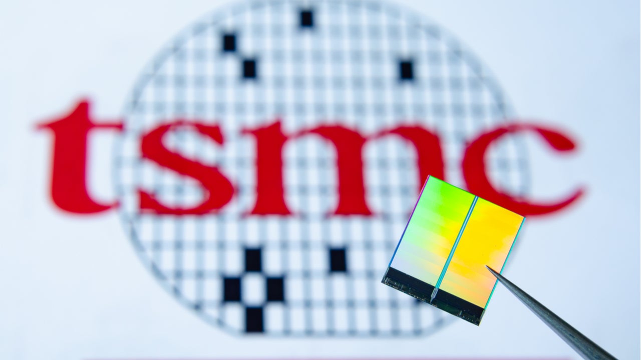
Taiwan Semiconductor Manufacturing Company (TSMC), the National University of Taiwan (NTU) and Massachusetts Institute of Technology (MIT) have jointly announced that a significant breakthrough was made in the development of 1-nanometer (nm) chips.
The research results published in the international journal Nature found that the use of semi-metal bismuth (Bi) as the contact electrode of the two-dimensional (2D) material can greatly reduce the resistance and increase the current. This can achieve energy efficiency close to the existing physical limits of semiconductor sizes.
Go deeper with GlobalData


Access deeper industry intelligence
Experience unmatched clarity with a single platform that combines unique data, AI, and human expertise.
According to the report, the discovery was first made by the MIT team, and then TSMC optimised the “easy deposition process.” NTU’s Department of Electrical Engineering and Optoelectronics successfully reduced the component channel through the helium ion beam lithography system.
The news follows IBM’s announcement earlier this month of its 2nm chip, which, according to IBM, will have 45% higher performance and use 75% less energy than today’s 7nm node chips.
For decades, chipmakers have put more transistors – the key components of microchips – onto ever smaller surfaces. This phenomenon, known as Moore’s law, posits that the number of transistors per unit area doubles about every two years.
However, chipmakers are now approaching the physical limit of the mainstream semiconductor material silicon, and the performance of the chip can no longer be significantly improved year by year.
In recent years, the scientific community has been actively searching for 2D materials that can replace silicon, challenging the manufacturing process below 1nm, but it has so far been unable to solve the problems of high resistance and low current of 2D materials.
According to the report, the research results could replace the next generation of chips and provide favourable outcomes such as power-saving and high speed. In the future, it is expected to be used in artificial intelligence, electric vehicles, disease prediction and other emerging technology applications.
However, it will likely take years before even 2nm semiconductors will become available in everyday devices. Today’s leading chips are 5nm, for example, and are only just appearing in premium smartphones.
TSMC has updated its latest semiconductor production roadmap in which it plans to start production of 4nm chips this year, while mass production should be achieved in 2022. Production of the 3nm chip will start in the second half of 2022. As for the future of TSMC, the company said that it would continue the development of 2nm and 1nm semiconductors.
According to GlobalData’s semiconductor sector scorecard, TSMC is the world’s largest chip foundry, making bespoke logic chips for companies that provide their own designs. The company, founded in 1987 and headquartered in Hsinchu, Taiwan, is one of the top ten thematic leaders in the industry.