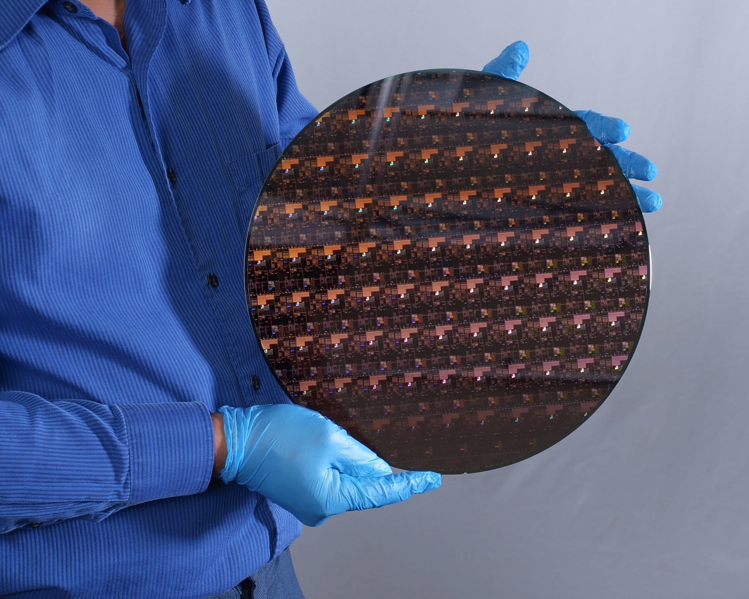
IBM has unveiled 2-nanometer chip technology that the tech giant says will provide performance and energy efficiency improvements for data centres, laptops, smartphones and other computing applications.
The 2-nanometer chip is based on IBM’s nanosheet technology and will hold up to 50 billion transistors on a chip “the size of a fingernail.”
Go deeper with GlobalData


Access deeper industry intelligence
Experience unmatched clarity with a single platform that combines unique data, AI, and human expertise.
The chip will have 45% higher performance and use 75% less energy than today’s 7-nanometer node chips, IBM said. These improvements could reduce the carbon footprint of data centres and improve smartphone battery life from charging daily to every four days.
However, it is likely to take several years before the 2-nanometer chips trickle through into devices. Today’s leading chips are 5-nanometers and are only just starting to appear in premium smartphones.
The extra computing muscle from the new chip technology could help power the next generation of edge computing, artificial intelligence and driverless cars.
For decades chipmakers have squeezed more transistors – the key components of microchips – onto ever smaller surfaces, doubling every two years. However, this phenomenon – known as Moore’s law – has recently slowed because the transistors are becoming so tightly packed that it is pushing the laws of physics to its limits.
As with 3-nanometer and 5-nanometer chips, the term 2-nanometer has no relation to the physical size of the microchip or any of its features and is instead a marketing term used to describe the next generation of chips. According to Venture Beat, IBM’s wafer measures 300 millimetres.
IBM does not make physical chips itself but continues to develop designs at its Albany NanoTech Complex research lab in New York. It outsources most of its manufacturing to companies such as Samsung.
“The IBM innovation reflected in this new 2-nanometer chip is essential to the entire semiconductor and IT industry,” said Darío Gil, SVP and director of IBM Research. “It is the product of IBM’s approach of taking on hard tech challenges and a demonstration of how breakthroughs can result from sustained investments and a collaborative R&D ecosystem approach.”
Chip designer and maker Intel plans to finalise designs for a 2-nanometer node in 2027.
The ongoing global chip shortage has highlighted the critical role semiconductors play in today’s economy. Nearly all automakers have been forced to pause production over a supply squeeze, while the latest generation of games consoles have struggled to meet demand.
Last week Apple and Samsung warned they expect to see an impact on sales due to the crisis. Executives of leading chip companies expect the shortage to continue into 2022.
“The scarcity of chipsets is driving up costs of not only the chipsets themselves, but even cheaper components of microchips, setting off panic buys (adding to the shortage) as well as increasing the cost of raw materials for consumer tech products,” noted GlobalData analysts in a report published this month.