IBM has announced the development of a semiconductor chip at the sub-1 nanometre scale, reaching the 0.7 nanometre (nm), or 7 angstrom, node.
The company states this is the first chip of its kind, as the sector seeks to address the ongoing challenges of traditional chip scaling.
Go deeper with GlobalData


Access deeper industry intelligence
Experience unmatched clarity with a single platform that combines unique data, AI, and human expertise.
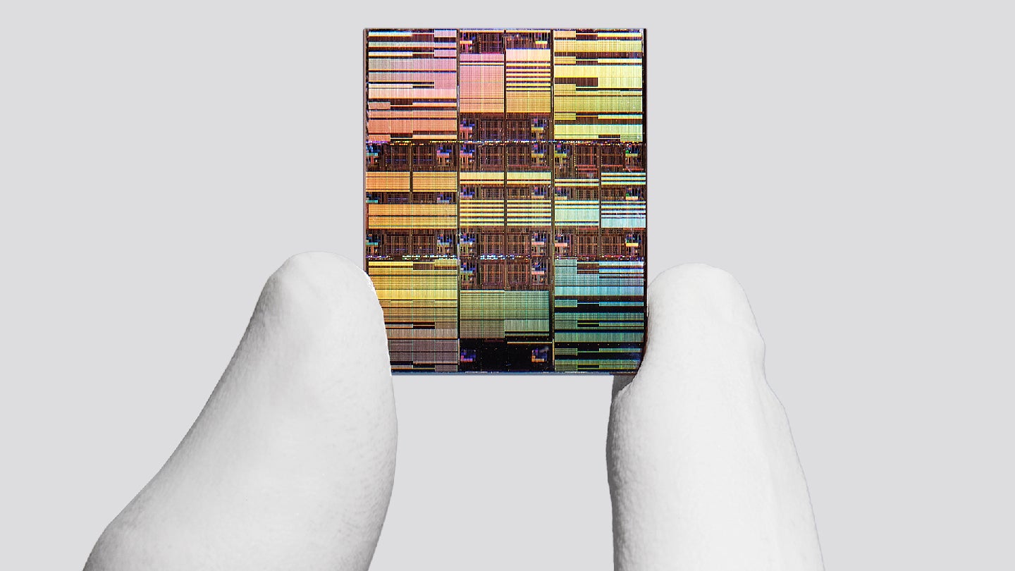
IBM reports that the chip integrates nearly 100bn transistors within a surface area similar to the size of a fingernail, almost double the density of its 2nm chip introduced in 2021.
The increase in density results from several changes in chip structure and materials, with a central role played by a three-dimensional nanostack architecture. According to IBM, this structural approach enables further progress in performance and efficiency as chip features approach atomic dimensions.
The company’s published data projects that the sub-1 nm chip could achieve up to 50% higher performance or 70% improved energy efficiency compared to IBM’s 2nm node chips. These figures are based on technical results set out in internal papers and presentations.
IBM highlights potential uses for workloads such as generative AI, cloud infrastructure, and new generations of electronic devices.
A primary feature of the chip is the nanostack transistor architecture, which IBM describes as the first three-dimensional, nanosheet-based design in the industry.
The design vertically stacks and staggers transistors using three-dimensional sequential integration. This setup allows for different materials to be used in each layer, which IBM states supports independent optimisation of both performance and power efficiency for every transistor.
IBM researchers report that they have validated the nanostack approach with experimental methods, including ultra-thin dielectric bonding within CMOS process integration and dual-channel engineering capabilities. They also demonstrated the operation of a functional CMOS inverter with expected switching performance.
According to IBM, these demonstrations confirm the physical feasibility of nanostack technology and its capacity for computation.
Additional research findings presented by IBM at the VLSI 2026 conference indicate that the nanostack design achieves a 40% improvement in area scaling for SRAM bitcells. IBM states that this area reduction supports more efficient chip designs and accommodates the high-bandwidth data requirements of advanced AI workloads.
The company notes that node descriptions now reflect manufacturing generations rather than exact measurements. IBM’s 0.7nm technology demonstrates that scaling can continue at the angstrom level.
The company projects its nanostack architecture could facilitate further chip density improvements for at least the next decade.
IBM Research director and IBM Fellow Jay Gambetta said: “IBM’s latest chip breakthrough marks a landmark moment in computing, pushing technology beyond the nanometer era to the scale of atoms. With our new nanostack architecture, we’re not just making smaller transistors, we’re reinventing how chips are built to deliver dramatically more power and energy efficiency.
“This industry-first innovation continues IBM’s legacy of leading in next-generation technologies and sets the foundation for the next era of computing.”
Development work for this chip took place at IBM’s research facility in Albany, New York. The site is expected to soon host a High Numerical Aperture Extreme Ultraviolet lithography tool from ASML, which IBM identifies as a necessary technology for future manufacturing nodes.
IBM, alongside partners Lam Research, Tokyo Electron, and SCREEN Semiconductor Solutions, has developed new High Numerical Aperture Extreme Ultraviolet (High NA EUV) processes that have resulted in working devices.
Furthermore, IBM has announced a plan to launch Anderon, described as a standalone quantum foundry. The company expects Anderon to focus on quantum wafer production, making use of IBM’s research in both quantum computing and semiconductors.
IBM has indicated that nanostack-based sub-1 nm technology could reach production within the next five years. The company sees the technology as supporting future computing domains that require increased transistor density and efficiency.
Earlier this year, IBM and Lam Research entered into a five-year agreement to develop new materials and fabrication processes aimed at enabling sub-1 nm logic scaling. Both companies are focusing on advancing High-NA EUV lithography processes and supporting the development of increasingly complex device architectures.